Fermi Level In Semiconductor : Fermi level of intrinsic and extrinsic semiconductors ... / Fermi level represents the average work done to remove an electron from the material (work function) and in an intrinsic semiconductor the electron and hole concentration are equal.
Fermi Level In Semiconductor : Fermi level of intrinsic and extrinsic semiconductors ... / Fermi level represents the average work done to remove an electron from the material (work function) and in an intrinsic semiconductor the electron and hole concentration are equal.. Fermi level is a kind of measure of equilibrium electronic energy of a solid material. The fermi level lies between the valence band and conduction band because at absolute zero temperature the electrons are all in the lowest energy state. The fermi level plays an important role in the band theory of solids. Fermi level is the state for which there is a 50% probability of occupation. Fermi level is the highest energy state occupied by electrons in a material at absolute zero temperature.
The fermi level is the surface of fermi sea at absolute zero where no electrons will have enough energy to rise above the surface. Position of fermi level in intrinsic semiconductors • width of conduction band and valence band is small as compared to forbidden energy gap. If you can bring the fermi level high enough, then part of the tail will go over to the conduction band. 1.1 0, indicating equal concentrations of electrons and holes. • at o k no conduction because at o k valence band is completely filled while conduction band empty and semiconductor behave as insulator.
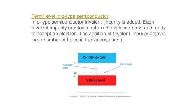
Difference Between P-Type and N-Type Semiconductor (with ... from electronicsdesk.com The fermi level plays an important role in the band theory of solids. Kb is the boltzmann constant. Of free electrons in conduction band. For the intrinsic semiconductor at 0k, is fermi energy and fermi level both are equal? Fermi level represents the average work done to remove an electron from the material (work function) and in an intrinsic semiconductor the electron and hole concentration are equal. The fermi level is referred to as the electron chemical potential in other contexts. Fermi level of extrinsic semiconductor extrinsic semiconductors are formed by adding suitable impurities to the intrinsic semiconductor. If you can bring the fermi level high enough, then part of the tail will go over to the conduction band.
Whenever the system is at the fermi level, the population n is equal to 1/2.
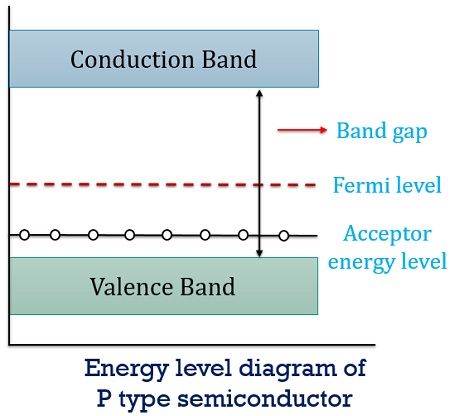
We mentioned earlier that the fermi level lies within the forbidden gap, which basically results from the need to maintain equal concentrations of electrons and holes. Semiconductor doping and higher temperatures can greatly improve the conductivity of the pure semiconductor material. Loosely speaking, in a p type semiconductor, there is. The added impurity is very small, of the order of one atom. 1.1 0, indicating equal concentrations of electrons and holes. Position of fermi level in intrinsic semiconductors • width of conduction band and valence band is small as compared to forbidden energy gap. The fermi level plays an important role in the band theory of solids. • at o k no conduction because at o k valence band is completely filled while conduction band empty and semiconductor behave as insulator. For si and ge, nc > nv and the correction term is negative while for gaas nc < nv and the correction term is positive. Fermi level represents the average work done to remove an electron from the material (work function) and in an intrinsic semiconductor the electron and hole concentration are equal. The fermi level is referred to as the electron chemical potential in other contexts. Of holes in valance band. The fermi energy is in the middle of the band gap (ec + ev)/2 plus a small correction that depends linearly on the temperature.
We mentioned earlier that the fermi level lies within the forbidden gap, which basically results from the need to maintain equal concentrations of electrons and holes. Fermi levels, forward bias prof j. The correction term is small at room temperature since eg ~ 1 ev while kbt ~ 0.025 ev. Smith context the first part of this lecture is a review of electrons and holes in silicon: The fermi level plays an important role in the band theory of solids.
Fermi Energy and Fermi Level - Definition and Applications ... from cdn1.byjus.com At absolute zero temperature intrinsic semiconductor acts as perfect insulator. As the temperature is increased, electrons start to exist in higher energy states too. Smith context the first part of this lecture is a review of electrons and holes in silicon: For si and ge, nc > nv and the correction term is negative while for gaas nc < nv and the correction term is positive. The fermi level is the surface of fermi sea at absolute zero where no electrons will have enough energy to rise above the surface. Due to lack of sufficient energy at 0 kelvin, the fermi level can be considered as the sea of fermions (or electrons) above which no electrons exist. Kb is the boltzmann constant. Smith department of eecs university of california, berkeley eecs 105 spring 2004, lecture 19 prof.
There are bands crossing the fermi level, so the material is metallic.
The fermi level lies between the valence band and conduction band because at absolute zero temperature the electrons are all in the lowest energy state. If you can bring the fermi level high enough, then part of the tail will go over to the conduction band. Of electrons in conduction band are greater than no. (a) fermi level position in pure semiconductors at this point, we should comment further on the position of the fermi levelrelative to the energy bands of the semiconductor. The fermi level plays an important role in the band theory of solids. Of free electrons in conduction band. Fermi level is the state for which there is a 50% probability of occupation. The fermi level is referred to as the electron chemical potential in other contexts. Whenever the system is at the fermi level, the population n is equal to 1/2. At absolute zero temperature intrinsic semiconductor acts as perfect insulator. Fermi levels, forward bias prof j. Ec is the conduction band. The electrical conductivity of the semiconductor depends upon the total no of electrons moved to the conduction band from the valence band.
The fermi level represents the electron population at energy levels and consequently the conductivity of materials. For si and ge, nc > nv and the correction term is negative while for gaas nc < nv and the correction term is positive. The fermi level lies between the valence band and conduction band because at absolute zero temperature the electrons are all in the lowest energy state. The fermi level is the energy separating occupied states of the valence band from empty states of the conduction band at the absolute temperature t=0 kelvin. As the temperature is increased, electrons start to exist in higher energy states too.
Fermi level in extrinsic semiconductor from image.slidesharecdn.com If you can bring the fermi level high enough, then part of the tail will go over to the conduction band. The fermi level represents the electron population at energy levels and consequently the conductivity of materials. Of free electrons in conduction band. The fermi level is at e / u = 1 and k t = u. • all energy level in one band is same energy. Kb is the boltzmann constant. The added impurity is very small, of the order of one atom. The correction term is small at room temperature since eg ~ 1 ev while kbt ~ 0.025 ev.
The correction term is small at room temperature since eg ~ 1 ev while kbt ~ 0.025 ev.
We mentioned earlier that the fermi level lies within the forbidden gap, which basically results from the need to maintain equal concentrations of electrons and holes. For si and ge, nc > nv and the correction term is negative while for gaas nc < nv and the correction term is positive. Smith department of eecs university of california, berkeley eecs 105 spring 2004, lecture 19 prof. Of electrons in conduction band are greater than no. Kb is the boltzmann constant. At absolute zero temperature intrinsic semiconductor acts as perfect insulator. The correction term is small at room temperature since eg ~ 1 ev while kbt ~ 0.025 ev. However as the temperature increases free electrons and holes gets generated. Fermi level is a kind of measure of equilibrium electronic energy of a solid material. Semiconductor doping and higher temperatures can greatly improve the conductivity of the pure semiconductor material. Of holes in valance band. Position of fermi level in intrinsic semiconductors • width of conduction band and valence band is small as compared to forbidden energy gap. As the temperature is increased, electrons start to exist in higher energy states too.


0 Komentar